Motivation

In recent years research at the nanoscale has exploded around graphene and other 2D materials, owing to their superior properties and extreme scale. Applying these novel materials to the 3D world, however, requires new and unique technologies. The objective of this program is the development, control and application of atomically thin, membrane-like integrated circuits and devices, which can fold, unfold, interact and communicate at the cellular/subcellular scale. Such ultrathin, substrate-free circuits will be over a 1,000 times more flexible and bendable than current flexible electronics, enabling folded, 3D structures with nanoscale features with previously unexplored mechanical, physical and surface properties. These novel properties offer revolutionary applications in health, biology, and remote and dispersable sensing with significant DoD relevance; examples include “wearable” and foldable electronics at the cellular and subcellular level, microscopic deployable structures whose surface area can increase by several orders of magnitude upon actuation, and aeroplankton-like deployable sensors that are aerosolized and dispersed in microscopic droplets.
Four Main Thrusts
-
How do we reliably fabricate, control and integrate atomically-thin metal, insulator, and semiconductor films to generate integrated circuits?

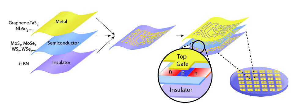
In Thrust I, our MURI team will address the scientific and engineering challenges to generate large scale 2DLM building blocks and 2DLM-ICs. We will first grow key 2DLM building blocks in large wafer scale, the (electrical, mechanical and surface) properties of which can be tuned during their growth. In particular, electrically insulating and semiconducting 2DLMs, whose large-scale availability is currently limited, will be produced. By patterning and assembling multiple 2DLM components using lateral stitching and vertical stacking, we will generate atomically-thin, substrate-free films including multiple, spatially distinct areas with different electrical, mechanical, and optical properties.This will serve two main purposes: first, it will enable us to fabricate and integrate a large array of devices, ultimately leading to the generation of 2DLM-ICs; second, it will provide large-scale 2DLM membranes with their properties spatially programmed, which is an ideal and necessary starting point for Thrust II and Thrust III. The large quantity of substrate-free 2DLM devices generated in Thrust I can be integrated with other materials platform and dispersed/deployed in liquid, thus enabling deployable and adaptable electronics and sensors.
-
Which mechanisms can be used to actuate their folding and unfolding to generate designed 3D structures?

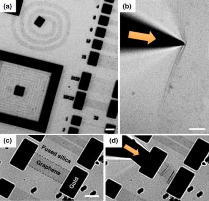
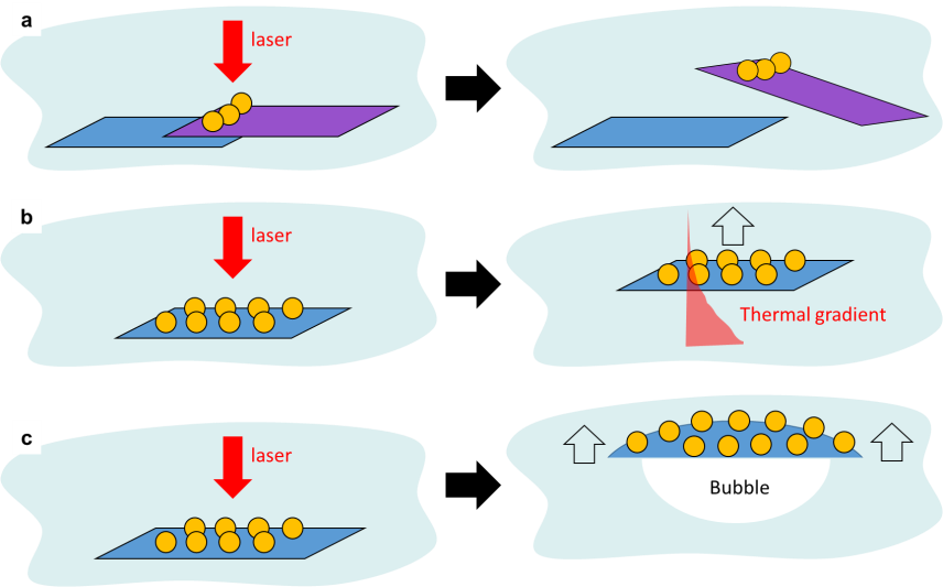
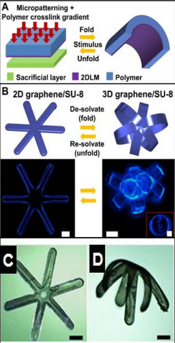
The challenge in Thrust II is to bend/fold the 2DLM membranes and devices described in Thrust I into the desired shape needed for deployment in a particular application.Our MURI team will develop a suite of general schemes to reversibly and controllably bend and fold atomically-thin 2DLM membranes. Our team has extensive experience with approaches to folding, bending and actuating small structures, including 2DLMs. These include: a. direct mechanical manipulation, b. optical and magnetic manipulation, c. bimorph actuators, and d. controlled surface tension.The work proposed here will adapt these approaches to the special needs/opportunities presented by 2DLM membranes. The work will encompass two distinct length scales. The first is the micron length scale, where our team has already used a variety of approaches, from optical manipulation to stimuli-responsive polymer films, to create new classes of configurable sensors and metamaterials. The second length is the nanometer scale. In order to curve membranes with nanoscale radii, we will utilize surface forces, which are extremely strong at small size scales, generating extraordinarily high strains thus bending the films with nanoscale radii.
-
How do we control, detect, and communicate with 2DLM devices remotely and wirelessly?

The fabrication of high performance integrated circuits with 2DLMs and their folding into compact shapes within ultra-small volumes offers the tantalizing prospect of substrate-free devices that can interact with biological systems with unprecedented sensitivity and dexterity. A major challenge faced in the practical deployment of these devices is to identify ways to “communicate” with them. How can we actively detect and actuate a mechanical motion within these devices, and how can we efficiently deliver electrical power? With untethered, mobile devices, conventional wire-based detection and actuation modalities are no longer viable. Remote solutions, such as those utilizing electromagnetic waves, are the only option.In this Thrust, our MURI team will address and innovate new scientific and engineering strategies towards communications with mobile 2DLM devices. The proposed concepts fall under three general approaches. The first is to explore how free-standing 2DLM devices, folded into 3D shapes, can function as morphology-dependent radio frequency (RF) device components. By coupling these devices to mechanically stretchable and reconfigurable RF antennas, their physical layouts can be detected and actuated. We will also explore how RF/optical energy can be converted to DC. The second approach is to understand how plasmonic nanostructures can couple to and enhance 2DLM devices. 2D materials are highly optically transparent due to their atomic-scale thickness, and their coupling with plasmonic structures can significantly enhance their interaction with light, with a variety of uses.
-
How do we generate and deploy functional, bendable 2DLM devices?

The ability to controllably and reversibly fold 2D materials on both a micron and nanometer scale(Thrust II), combined with the integrated functionality discussed in Thrust I and the communications strategies in Thrust III, opens up many possibilities for novel devices. One of our main visions for membronic 2DLM device integration is to remotely actuate the chemical, mechanical, and electrical state of 2DLM devices using RF digital communications. Digital RF signaling is the standard communications protocol used with modern mobile and embedded systems, and their adaption to free standing 2DLM devices will significantly expand their scope of operation and application, and take advantage of already existing technology platforms. Most generally, our goal in Thrust IV is to integrate Thrust I, Thrust II, and Thrust III to mass-produce large quantities of foldable micro and nanostructures composed of 2DLMs that can be dispersed in aqueous environments.


