Motivation:
 The critical features in electronic devices are approaching atomic dimensions. In addition, the device structures have become 3D and more complex in their geometry. Consequently, the development of techniques that can provide atomic scale precision in these geometries is very desirable.
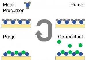
Atomic layer deposition (ALD) has exhibited the ability to grow uniform and conformal thin films of controlled thickness and composition. If methods can be developed to produce selective growth, ALD can help solve emerging challenges in patterning.
Coupled microreactor/UHV surface analysis:
We are investigating the mechanisms involved in new methods that could be employed to achieve area selective deposition using ALD.
Experiments are performed in a custom-built ultra-high vacuum (UHV) chamber:
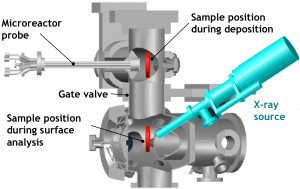 – Designed for surface modification and thin film deposition
– Enables reactions followed by in vacuo transfer of sample to chamber for in situ X-ray analysis
– Multiple inlets for independent exposure of up to 3 reactants
– Cylindrical reaction zone (dia. ~ 1.5 cm)
– Effluent grooves confine reactant gas and preserve UHV environment (dia. ~ 3 cm)